Project Description

Task:
Convert a four page product outline of a telecom measurement card featuring 8 fiber optic links, the largest Xilinx Virtex FPGA to date, four instances of fast QDR memory into a functional PCIex8 card prototype hardware in less than 8 weeks.
Challenges:
- Very quick turn project time line
- Huge device package uses up almost the entire card height (FGG1760) on low profile PCIe card
- Huge power budget for an LX330T
- Wide buses to memory
- Fast MGT signals zu optical block and PCIe X8
- Configuration time of LX330T to meet PCIe reset timing
Solutions:
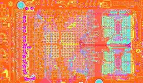
To implement a design with such high signal density and such wide buses with a reasonable amount of PCB layers, the signal allocation on the FPGA, especially on the wide memory buses, had to be optimal in order to limit the amount of signals that need to cross. Only because Knowledge Resources designers posses in depth FPGA knowledge and advanced Layout skills, could this design with its countless layout, pin-swap back to layout iterations, be competed in such short time.
The final solution consisted of a 12 layer PCB stack with two tiers of staggered laser micro-vias per side. A layer stack with split planes and re-allocated plane layers allowed for the routing of all the signals, provided ample space for length matching and impedance controlled traces for fast signals.
The power management needs were addressed by fully encapsulated POL regulators with multiple modules sharing the load of the core FPGA supply. since all POL regulators operated off a common, but phase shifted clock, input bypass capacitance needs could be reduced and EMI emissions minimized.
The required maximum configuration time was achieved by using a dedicated wide configuration solution running at 50 MHz
Technologies used:
– Layout experience coupled with in-depth FPGA knowledge, Xilinx Virtex5 LX330T, PCIe, Synchronous POL regulators, QDR memories

