SO, since our first attempt of creating the “perfect” FPGA module was quite successful, we decided to try and do even better. Not that the KRM1k modules don’t have their place, but time (and therefore technology) progresses and the features that are now available in the 7 series parts from Xilinx could simply not be encapsulated in a SO-DIMM form factor module and at the same time be fully accessible by the system designer.
I quickly re-iterate the original two driving rules for a Knowledge Resources FPGA module design:
…the modules only carry features that are required in every design.
- Core power supply
- Configuration memory
- Reset and proper initialization
features are also included if they add significant complexity to the design if they had to be implemented on the carrier.
- DDR memories
- Use of small pitch & high I/O count FPGA packaging
Sticking to those rules has served us well with the KRM1K module but we feel that there is always room for improvement so we are adding the following rules before starting the design of the next generation:
Rule #3
… A module may not limit access to key features of an FPGA family
- MGT’s must be accessible
- Processing subsystem pins must be accessible
Rule #4
… I/O signals on a module connector must be as universally usable as possible
- Bank voltages must be flexible and decided by the end use design not the module
- Signals must be length matched between FPGA and carrier board interconnect to allow for fast buses
- Signals should be available on “board down” connectors and not via extra flex cables whenever possible
Rule #5
… Modules should provide a fully compatible upgrade path between FPGA members and families
- Byte groups (T0-T3) must be mapped consistently on all module variants
- A Kintex module variant must be able to provide MIO features of a Zynq variant via soft cores
- Dedicated MGT lanes must be reserved
- A common heat management specification, with consistent build envelope, must exist
In defining the KRM3k specification, we listed to our own wishes, and why not?
KRM3k modules feature the following common external features:
- 70mm x 50mm , 5mm or 4mm spacing to carrier (connector choice in end-user design)
- Heat spreader for a total build height of 10mm or 11mm (depending on connector choice)
- 4×48 bit PL GPIO (192 GPIO signals, 96 diff pairs)
- the entire MIO_1 signal range
- up to 8 MGT lanes with 2 MGT ref-clock inputs
- JTAG
- Config done OC output
- Reset input
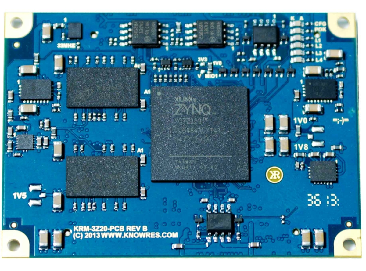
The first product that is based on this specification is the KRM-3Z20-512 board. It features:
- Xilinx Zynq XC7Z020-1CLG484C
- 2 Instances of 128Mb x16 LP DDRIII RAM @667MHz (512MB total)
- 256Mb config memory, two times 4X SPI memory
- 4 application status LED
I think we did it… it is perfect (at least until we come up with something even better..) 😉