A Selection From Our Projects
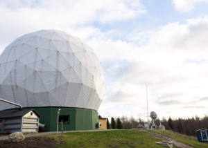
KRM-4 used in the world’s widest bandwidth radio astronomical receiver
Metsähovi Radio Observatory uses KRM-4 in the world’s widest bandwidth radio astronomical receiver Photo by Mikko Raskinen Researchers [...]
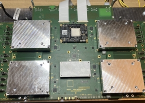
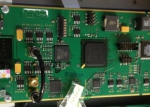
IAF – KRM-4 Broadband 8-channel SDR transceiver
IAF - KRM-4 Broadband 8-channel SDR transceiver IAF GmbH in Braunschweig, Germany uses our RFSoMs KRM-4ZU47DR or KRM-4ZU48DR in their [...]
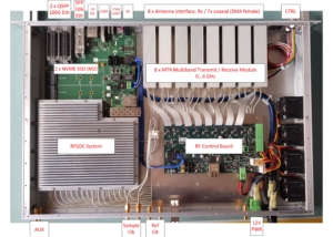
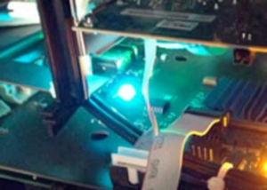
RF – test platform utilizing four KRM-4 RF-SoC modules
RF Test system featuring four RFSoC Modules To automate the testing of a very complex RFSoC carrier design, [...]
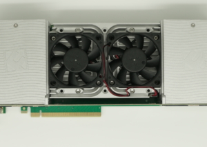
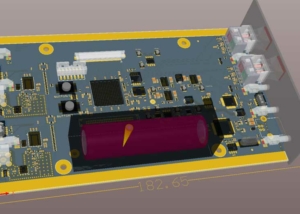
Multi FPGA compute acceleration PCIe card
Multi FPGA PCIe acceleration card with sizeable non volatile storage
Robot Swarm
A swarm of custom robots with a novel precision optical tracking system and real time image processing in FPGA
OFDM SDR Radio front end
OFDM SDR Radio Front End design with high speed converters and extremely low jitter requirements
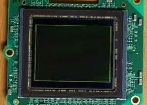
50 MegaPixel Image-Sensor Evaluation Platform
Evaluation of the optical and electrical characteristics of a mid- format 50 Megapixel CMOS image sensor.
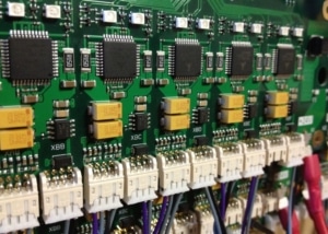
48 Channel Motor Control
FPGA based 48 Channel Motor and actuator control with tight time synchronization
ISM Band Radio Modem with POF link
Dual Channel full duplex ISM band RF modem with FPGA based data router and Plastic optical fiber data link
LOW LATENCY FIBEROPTIC VIDEO & DATA LINK
Low latency Fiber-optic Data & Video link with 2 microsecond round trip latency for data packets
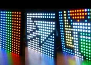
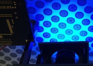
LED color video panels
LED video panel tiles, scalable, deep color, 600Hz refresh rate